Market Summary and Growth Forecast
The global Copper nanoparticles Market is estimated at $118.2 million in 2026 and is expected to reach $284.6 million by 2035, growing at a CAGR of 10.3%.
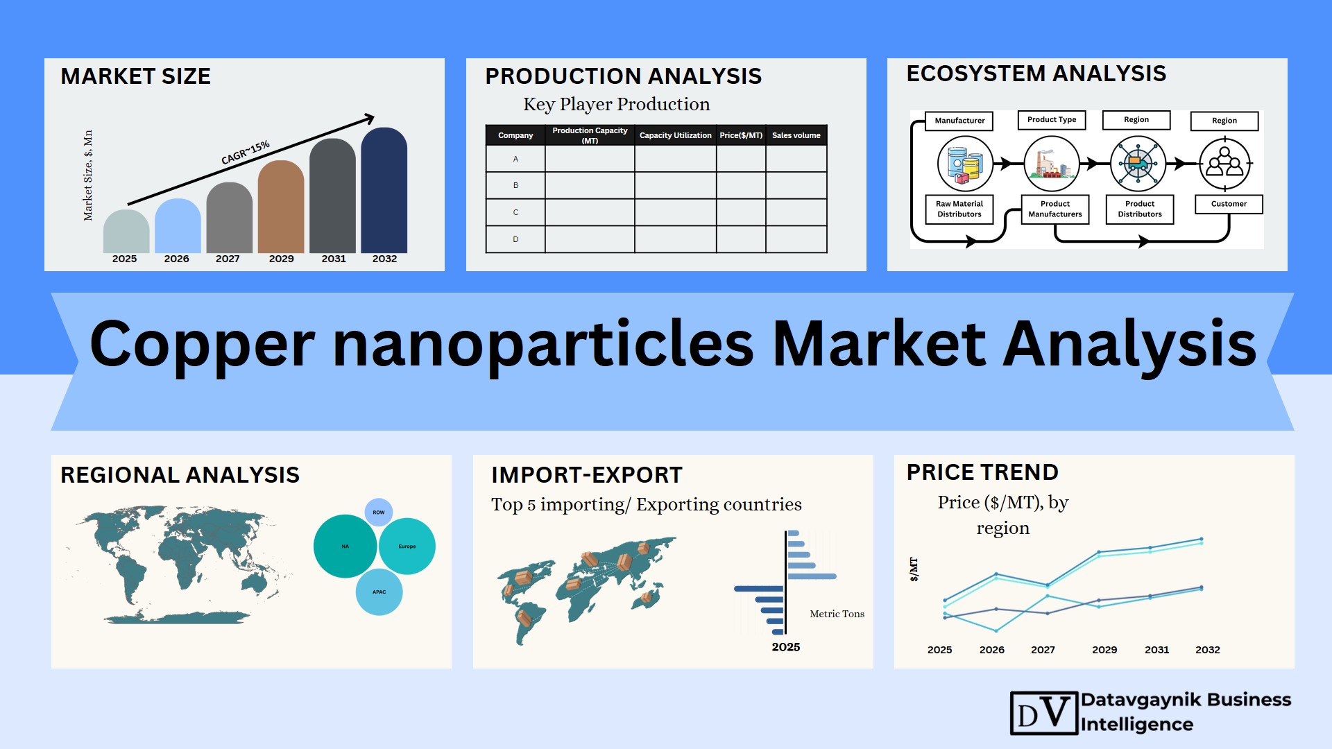
These figures are original analyst estimates. The model combines estimated commercial shipment volumes, industrial selling prices, application-grade premiums and expected adoption across electronics, coatings, catalysis and energy materials. It does not use published market sizes from syndicated market research companies.
Datavagyanik also covers related markets such as the Copper Nanoparticles in Antimicrobial Coatings Market, the Silica nanoparticles Market, and the Zinc oxide nanoparticles Market. These materials are considered in high-temperature and specialty chemical environments, where glass production, catalysis, and safety regulations influence adoption patterns.
| Market indicator | 2026 estimate | 2035 forecast |
| Global market revenue | $118.2 million | $284.6 million |
| Commercial shipment volume | 1,480 metric tons | 4,180 metric tons |
| Average realized price | $79.9 per kg | $68.1 per kg |
| Revenue CAGR | — | 10.3% |
| Volume CAGR | — | 12.2% |
The Copper nanoparticles Market covers elemental copper particles that are generally produced within the nanoscale range and sold as dry powders, stabilized dispersions, concentrates, pastes or conductive formulations. The commercial boundary includes the value of copper nanoparticles and nano-copper formulations supplied to industrial users. It excludes conventional micron-sized copper powder, copper nanowires, copper oxide nanoparticles and the revenue generated from finished electronic devices.
This distinction matters. Copper oxide nanoparticles have different electrical, catalytic and biological characteristics. They also serve a partly different customer base. Combining the two would inflate the addressable market and distort pricing.
Why the market matters
Copper nanoparticles sit between commodity copper and specialty functional materials. The raw metal is widely available. The value is created by controlling particle size, purity, surface chemistry, oxidation resistance and dispersion stability.
At the nanoscale, copper offers high electrical and thermal conductivity along with useful catalytic and antimicrobial properties. It can also replace part of the silver used in printed electronics, photovoltaic metallization and conductive pastes. Copper’s lower material cost makes the substitution commercially attractive. The challenge is that copper oxidizes more readily than silver. Even a thin oxide layer can increase electrical resistance and reduce product reliability.
So, the business case is not simply “copper is cheaper.” Suppliers must deliver copper that remains stable during storage, printing, curing and final use. The companies that solve this problem can participate in much larger downstream markets without competing directly with bulk copper producers.
Technology and application forces
The largest demand pool comes from conductive materials used in printed and flexible electronics. Copper nanoparticles can be formulated into inks and pastes for antennas, sensors, printed circuits, heaters, electrodes and electronic packaging. Recent technical work has demonstrated flexible nano-copper circuits produced through direct ink writing and low-temperature sintering. Laser-based processing is also being developed to create conductive copper tracks on temperature-sensitive polymer substrates without heating the entire component.
Photovoltaic metallization is becoming an important strategic opportunity. Solar cells have traditionally used silver in conductive contacts. Rising silver consumption and cost exposure are pushing manufacturers to test copper-rich and silver-free systems. In September 2025, TNO reported a screen-printing process that applied copper electrodes to silicon heterojunction solar cells while producing electrical output close to silver-metallized cells.
Demand will also come from:
- Catalyst manufacturers, particularly those developing materials for chemical reactions, environmental treatment and hydrogen-related processes.
- Antimicrobial coating formulators serving healthcare surfaces, textiles, polymers and high-contact industrial products.
- Battery and energy-material developers using copper nanoparticles as conductive additives, surface modifiers and components of experimental electrode systems.
- Thermal-material suppliers producing conductive adhesives, interface materials and specialized metal-polymer composites.
- Research laboratories and universities purchasing high-purity material for formulation and application development.
Copper nanoparticles are unlikely to replace silver in every conductive application. Silver remains easier to process and more resistant to oxidation. Copper is more likely to penetrate products where material cost, printing speed and high-volume manufacturing are more important than maximum conductivity under every condition.
Production economics
Commercial copper nanoparticles are produced through chemical reduction, polyol processing, electrochemical routes, plasma-based production, gas-phase condensation and other physical or chemical techniques. No single process is ideal for every grade.
Chemical processes can offer good particle-size control and relatively flexible surface treatment. However, they require careful removal of residual solvents, reducing agents and stabilizers. Physical processes can produce high-purity material but may involve higher equipment and energy costs.
The main production variables are:
- Particle-size distribution
- Metallic copper content
- Surface oxide concentration
- Particle morphology
- Agglomeration control
- Dispersibility
- Batch consistency
- Storage stability
- Production yield
These variables explain the wide difference between the price of standard nano-copper powder and application-ready material. A formulation qualified for inkjet printing or fine-line photovoltaic metallization can command a much higher price than general-purpose powder.
The market model assumes that average realized prices will decline from $79.9 per kg in 2026 to $68.1 per kg in 2035. This does not mean every grade becomes cheaper. High-purity and customized formulations will retain strong pricing. The decline reflects larger production batches, better yields and a higher contribution from high-volume industrial material.
Regulatory and safety considerations
Nanomaterial regulation will shape supplier selection. In the European Union, explicit REACH information requirements for nanoforms have applied since 2020. Registrants may need nanoform-specific characterization, hazard information and exposure documentation. Safety data sheets must also communicate relevant nanoscale characteristics.
In the United States, nanoscale materials can fall under Toxic Substances Control Act reporting and recordkeeping requirements. This makes particle characterization and production records important for suppliers entering regulated industrial supply chains.
The regulatory effect will be uneven. Electronics applications usually encapsulate the material within a cured conductive track. Loose powders create a different handling profile. As a result, many customers will prefer pre-dispersed or paste-based products that reduce airborne particle exposure during manufacturing.
Key consumers and client groups
The principal customer groups are:
- Conductive ink and electronic paste formulators
- Printed circuit and flexible electronics manufacturers
- Semiconductor packaging and electronic component companies
- Photovoltaic cell and module producers
- RFID and smart-label converters
- Sensor and wearable-device manufacturers
- Industrial catalyst producers
- Antimicrobial coating and polymer compounders
- Battery-material and energy-storage developers
- Universities, national laboratories and nanotechnology research centres
For decision-makers, the Copper nanoparticles Market should be viewed as a qualification-led specialty material business. Commercial success depends on more than production capacity. Suppliers need application laboratories, formulation capability and close technical engagement with customers.
Expert view: The leading suppliers will not necessarily be those with the lowest powder price. The stronger position will belong to companies that can guarantee oxidation control, dispersion stability and repeatable performance after printing or curing.
Market Segmentation and Forecast Scope
The Copper nanoparticles Market is segmented by product form, application, end user and region. The segmentation is designed to avoid overlap. Revenue is assigned according to the form in which the material is sold and the primary application for which it is purchased.
By Product Type
| Product type | Scope and commercial role | 2026 position | Forecast direction |
| Dry copper nanopowder | Unformulated metallic copper nanoparticles supplied for customer-side mixing, research, catalysis, compounding and formulation | 52.8% share, equal to $62.4 million | Remains the largest product category by revenue |
| Stabilized copper nanoparticle dispersions | Nanoparticles dispersed in water, alcohols, glycols or organic carriers with surface stabilizers | Share not disclosed | Gains adoption where dust control and formulation consistency matter |
| Nano-copper pastes and inks | Application-ready conductive formulations for screen, inkjet, aerosol, direct-write and other printing processes | Share not disclosed | Fastest-growing product type at an estimated 12.7% CAGR |
Dry copper nanopowder holds the largest share because it serves several applications and can be customized by downstream formulators. It is also widely supplied in research and pilot-production quantities.
That said, value creation is moving toward stabilized dispersions and nano-copper pastes and inks. Customers increasingly want materials that already meet viscosity, surface tension, particle-loading and curing requirements. This reduces formulation time and lowers the risk of agglomeration during production.
Application-ready inks will generate the fastest growth. They are harder to qualify but create a stronger customer relationship once approved. A supplier that becomes part of a customer’s printing and curing process is also less exposed to price-based replacement.
By Application
| Application | Included uses | 2026 position | Strategic outlook |
| Electronics and conductive formulations | Printed circuits, RFID antennas, sensors, heaters, electrodes, component interconnects and packaging materials | 42.5% share, equal to $50.2 million | Largest and most commercially developed application |
| Catalysis and chemical processing | Supported catalysts, reaction promoters and environmental treatment materials | Share not disclosed | Stable industrial demand with formulation-specific opportunities |
| Antimicrobial materials and coatings | Functional coatings, polymers, textiles and surface-treatment systems | Share not disclosed | Growth moderated by safety, efficacy and registration requirements |
| Energy storage and conversion | Conductive additives, electrode modification, experimental batteries, fuel cells and photovoltaic metallization | Share not disclosed | Fastest-growing application at an estimated 13.6% CAGR |
| Thermal materials and other specialty uses | Thermal interfaces, conductive composites, research materials and niche functional products | Share not disclosed | Selective growth based on performance requirements |
Electronics and conductive formulations are the largest application because conductivity is copper’s clearest commercial advantage. Printed electronics suppliers are working to reduce their reliance on silver. Copper allows lower material cost but requires better protection from oxidation.
Energy storage and conversion will grow faster from a smaller base. The segment includes copper-enabled electrode structures, conductive additives and photovoltaic contacts. Recent research has also examined copper-decorated silicon particles as a conductive alternative in lithium-ion battery anodes. The material improved electrode conductivity and showed benefits in capacity retention and rate performance in laboratory testing.
Not every laboratory result will translate into commercial volume. Battery qualification cycles are long. The more immediate revenue opportunity lies in photovoltaic contacts and printed power-management components.
By End User
| End-user group | Purchasing requirement | 2026 position | Growth assessment |
| Electronics and electrical-material companies | Conductivity, fine-line printing, substrate compatibility and reliability | 44.1% share, equal to $52.1 million | Largest end-user category |
| Solar, RFID and printed-product converters | High-speed printing, low metal consumption and acceptable curing temperatures | Share not disclosed | Fastest-growing customer group |
| Chemical and process industries | Surface area, catalytic activity, purity and repeatable particle characteristics | Share not disclosed | Moderate and technically diverse demand |
| Healthcare, coatings and polymer companies | Antimicrobial performance, dispersion safety and regulatory documentation | Share not disclosed | Selective adoption |
| Research and institutional customers | Small lots, high purity and broad grade availability | Share not disclosed | Important for product development but limited in industrial volume |
Electronics and electrical-material companies account for the largest end-user share. This includes conductive material formulators as well as manufacturers integrating nano-copper into components.
Solar, RFID and printed-product converters are expected to expand at approximately 12.3% annually through 2035. Their purchasing criteria are different from those of research customers. They need stable industrial lots, high throughput and compatibility with existing printing equipment.
By Region
| Region | Market characteristics | 2026 position | Forecast outlook |
| North America | Strong nanomaterial research, advanced electronics, aerospace, defence and specialty material demand | Share not disclosed | Estimated 10.0% CAGR |
| Europe | Printed electronics, automotive systems, industrial coatings, solar R&D and stricter nanoform documentation | Share not disclosed | Estimated 9.5% CAGR |
| Asia Pacific | Large electronics supply chain, nanopowder production base, solar manufacturing and expanding printed-electronics capacity | 47.3% share, equal to $55.9 million | Fastest regional expansion at 10.9% CAGR |
| LAMEA | Research-led adoption, imported specialty material and selective industrial demand | Share not disclosed | Estimated 8.4% CAGR |
Asia Pacific leads the Copper nanoparticles Market because the region combines upstream material production with a large downstream electronics and photovoltaic manufacturing base. China, Japan and South Korea are central to supply. Taiwan also contributes through its electronics and material-processing ecosystem. India is smaller but is building demand through electronics manufacturing, specialty chemicals and research institutions.
North America remains important for high-value grades, intellectual property and early-stage qualification. Demand is concentrated in printed electronics, aerospace systems, sensors, research and specialized energy materials.
Europe will focus more heavily on process safety, traceability and lower-impact production. This may slow the qualification of poorly documented suppliers. It can also favour companies able to provide detailed material characterization and lifecycle information.
LAMEA remains an emerging opportunity. Brazil, Israel, the United Arab Emirates and selected South African institutions represent the more visible demand centres. Most material will continue to be imported during the forecast period.
Expert view: Dry powder will remain important. However, the profit pool will move toward stabilized and application-ready products. By 2035, formulation knowledge will carry more commercial weight than nominal nanoparticle production capacity.
Market Trends and Innovation Landscape
Innovation in the Copper nanoparticles Market is moving from basic particle synthesis toward full process compatibility. Earlier work focused on producing smaller and purer copper particles. Current development is more practical. Customers want material that survives storage, prints cleanly, cures quickly and maintains conductivity during use.
Oxidation-resistant particle engineering
Oxidation remains the central technical issue. Copper nanoparticles have a high surface-area-to-volume ratio. This makes them reactive. The oxide layer formed during production or storage can interfere with particle-to-particle contact during sintering.
Suppliers and research groups are addressing this through:
- Organic ligand passivation
- Polymer and surfactant coatings
- Copper–silver core-shell structures
- Copper–nickel protective shells
- Reducing additives
- Oxygen-controlled packaging
- Self-reducing ink chemistry
- Encapsulation systems that decompose during curing
Core-shell particles provide one possible route. A thin protective layer can reduce oxidation while preserving the cost advantage of a copper-rich core. Copper–silver core-shell pastes have already been studied as lower-cost alternatives to silver-rich conductive pastes.
The commercial balance is delicate. Too much surface coating can interfere with conductivity. Too little protection results in poor shelf life. Product development is therefore shifting toward application-specific surface chemistry rather than one universal copper nanoparticle grade.
Lower-temperature and faster sintering
Traditional thermal sintering can damage polymer films, paper, textiles and other flexible substrates. It can also limit line speed. The industry is testing localized and rapid-energy processes that join copper nanoparticles without heating the entire substrate.
Important methods include:
- Intense pulsed-light processing
- Laser sintering
- Photonic curing
- Microwave-assisted sintering
- Chemical sintering
- Plasma treatment
- Formic-acid and reducing-atmosphere processing
A 2025 study demonstrated laser sintering of copper ink as an alternative to oven processing. Localized heating helped protect low-melting polymer substrates such as PET.
Low-temperature processing has a direct commercial impact. It opens demand in smart packaging, wearable sensors, disposable diagnostics and flexible electronic assemblies. It can also reduce manufacturing time.
Expert view: The next performance benchmark will not be conductivity alone. Customers will compare conductivity, curing temperature, processing speed, shelf life and substrate damage as one combined value proposition.
Shift toward application-ready formulations
Customers are moving away from buying nanoparticles as isolated laboratory materials. They increasingly prefer formulations designed for a specific printing or deposition technique.
Inkjet systems require low viscosity and tight control of particle size to prevent nozzle blockage. Screen printing needs higher viscosity and controlled thixotropy. Aerosol printing requires stable atomization. Photovoltaic metallization needs fine lines, strong adhesion and low contact resistance.
This is changing supplier strategy. Nanoparticle manufacturers are adding dispersion and formulation capability. Ink companies are developing closer relationships with particle producers. Some businesses are integrating inks, printing equipment and curing processes into a single offer.
The model therefore forecasts nano-copper pastes and inks as the fastest-growing product category. Their growth will exceed that of general-purpose powder even though powder remains the larger category in 2026.
Silver substitution in photovoltaic and printed electronics
Silver replacement is becoming one of the strongest innovation themes. Copper offers a lower-cost conductive metal base. It is also widely available and recyclable. However, successful substitution requires compatible printing, curing and contact-protection processes.
In September 2025, TNO announced copper-electrode silicon heterojunction solar cells produced through screen printing. The development showed that copper-based metallization could approach the electrical output of conventional silver systems.
In March 2026, Copprint announced a fourth-generation conductive copper ink intended for ultra-fine lines and photovoltaic applications. The product direction reflects the move toward narrower printed features and lower metal consumption.
Hybrid systems will remain relevant. In October 2025, NovaCentrix introduced a family of silver-coated copper inks positioned as a lower-cost alternative to high-silver formulations. Such products reduce silver consumption without requiring an immediate move to fully uncoated copper.
Continuous and more sustainable manufacturing
Industrial customers need larger batches with narrow particle-size distributions. Batch chemical reduction can deliver good material but may create variation between production runs. Continuous-flow synthesis, improved precursor mixing and inline particle monitoring are therefore becoming more important.
Water-based and lower-solvent formulations are also receiving attention. They can reduce volatile organic compound exposure and simplify workplace controls. Still, water-based copper systems are technically difficult because water can accelerate oxidation unless the particle surface and formulation environment are carefully managed.
Production sustainability will increasingly be measured through:
- Solvent consumption
- Reducing-agent selection
- Energy use
- Metal yield
- Wastewater generation
- Recovery of off-specification copper
- Packaging stability
- Worker exposure
The value of these improvements will be strongest in Europe and in multinational electronics supply chains where suppliers are asked to provide environmental and chemical-management documentation.
Catalysis and energy-material research
Copper nanoparticles provide active surface sites for chemical reactions. Researchers are evaluating them in hydrogenation, carbon dioxide conversion, environmental treatment and electrochemical processes.
Energy-storage research is also expanding. A 2025 study examined copper nanoparticles assembled on zinc foil and processed through rapid laser annealing. The resulting copper–zinc surface helped control dendrite formation and supported longer cycling in a zinc-based battery configuration.
These developments support long-term demand. Yet electronics will commercialize faster because nano-copper already has a clear functional role as a conductor. Catalytic and battery applications often require additional testing around reaction stability, material recovery and long-term electrochemical behaviour.
Safe-by-design development
Regulation is pushing product development toward better characterization. Customers need more than a nominal particle-size claim. They may request information on number-based particle distribution, morphology, surface coating, solubility, agglomeration and exposure conditions.
Since explicit nanoform requirements under REACH have applied from 2020, European suppliers and importers face clearer obligations to document relevant nanoforms and their safe use.
This will favour suppliers with strong analytical capability. Smaller producers may offer competitive prices but struggle to support multinational customers if their documentation is incomplete.
Partnerships, product announcements and industry activity
Pure-play merger and acquisition activity remains limited. The observed pattern is partnership-led commercialization. This is logical. Application qualification requires close cooperation between nanoparticle suppliers, ink formulators, printing-equipment providers and end users.
| Date | Company or organization | Development | Market implication |
| September 2024 | Nanohmics and NovaCentrix | Announced a strategic collaboration in flexible microwave electronics | Shows how material and application engineering are being combined |
| February 2025 | ISC Konstanz, FuturaSun and Copprint | Advanced copper-screen-printed photovoltaic technology toward manufacturing | Supports the use of nano-copper formulations in solar metallization |
| May 2025 | Daio Engineering, Tatsuta Electric Wire and Daio Paper | Developed a paper-based RFID tag using copper nano ink | Demonstrates commercial potential in recyclable and security-focused smart labels |
| September 2025 | TNO | Reported copper-electrode silicon heterojunction solar cells | Strengthens the technical case for reducing silver use in solar cells |
| October 2025 | NovaCentrix | Introduced silver-coated copper conductive inks | Provides a transitional route between silver-rich and fully copper-based systems |
| March 2026 | Copprint | Released a copper ink for ultra-fine lines and photovoltaic applications | Indicates movement toward higher-resolution and higher-volume printing |
The ISC Konstanz–FuturaSun initiative uses copper-based metallization in advanced solar-cell designs, while the Daio Engineering–Tatsuta Electric Wire–Daio Paper development applies copper nano ink to paper RFID tags. These are relevant because they move nano-copper beyond material testing and into specific manufactured products.
The lack of major consolidation should not be interpreted as weak interest. The market remains technically fragmented. Suppliers often specialize in synthesis, dispersion, printing or curing. Partnerships allow each company to retain its intellectual property while sharing the qualification burden.
Innovation outlook through 2035
Three innovation paths will shape the market through 2035.
First, oxidation protection must become reliable under normal industrial handling. Customers will not adopt copper simply because laboratory samples perform well immediately after production.
Second, curing temperatures must fall further. This will increase compatibility with paper, polymer film, textiles and low-cost flexible substrates.
Third, suppliers must offer manufacturing-level consistency. Particle size, surface composition and rheology need to remain stable across large production lots.
The Copper nanoparticles Market will therefore become less dependent on the sale of generic powders. More revenue will come from tailored dispersions, conductive formulations and technical support. The winning products will be designed around a customer process rather than sold as isolated nanomaterials.
Expert view: Copper nanoparticles are moving from an interesting silver substitute to a process-engineered conductive platform. The transition will be gradual. Once a formulation proves reliable at production speed, however, the cost advantage can support rapid volume expansion.
Competitive Intelligence and Benchmarking
Competition in the Copper nanoparticles Market remains fragmented. No supplier controls the complete value chain. Some companies specialize in high-purity powders. Others focus on stabilized dispersions, conductive inks or application engineering.
This creates two distinct competitive groups.
The first group sells copper nanoparticles as an advanced raw material. Its customers include research laboratories, coating formulators, catalyst developers and industrial material companies. Product purity, particle size and surface treatment drive supplier selection.
The second group sells formulated conductive materials. These companies compete through printing performance, curing conditions, oxidation control and final electrical conductivity. Their customer relationships are usually deeper because formulations must be qualified within a specific production process.
Competitive Benchmarking Table
| Company | Primary market offering | Market position | Key competitive strength | Main commercial constraint |
| American Elements | High-purity copper nanopowders and dispersions across several particle-size ranges | Broad global specialty-material supplier | Large material catalogue and ability to support research and industrial procurement | Less focused on complete printed-electronics process integration |
| Hongwu International Group | Copper nanopowders, coated particles, dispersions and customized formulations | Cost-competitive Asian manufacturing specialist | Broad particle-size availability and customization for bulk orders | International qualification and regulatory documentation may vary by customer requirement |
| Nanoshel | Partially passivated copper nanoparticles and general-purpose nanopowders | Global research and pilot-scale supplier | Easy access to small quantities and a wide engineered-material portfolio | Limited visibility in high-volume conductive-ink qualification |
| Nanografi | High-purity spherical copper nanopowders and related advanced materials | Research-led European and international supplier | Strong positioning in universities, laboratories and advanced-material development | Industrial-scale copper formulation presence remains less developed |
| US Research Nanomaterials | Copper nanopowders for conductive coatings, additives and specialty applications | Established North American nanomaterial catalogue supplier | Wide selection of metals, alloys and oxide nanoparticles | Primarily material-led rather than application-system-led |
| NovaCentrix | Conductive inks, silver-coated copper formulations and photonic curing technologies | Advanced printed-electronics solution provider | Combines formulation knowledge with rapid curing and process equipment | Current copper positioning includes hybrid silver-coated systems rather than only pure copper |
| Copprint | Pure nano-copper inks for photovoltaics, printed circuit boards, antennas and fine conductive lines | Focused copper-ink commercialization specialist | Strong silver-substitution proposition and application-specific formulation development | Scaling depends on customer qualification and industrial production adoption |
American Elements
American Elements operates as a broad specialty-material supplier rather than a copper-only producer. Its copper portfolio includes high-purity nanoparticles in different particle-size ranges as well as copper nanoparticle dispersions in water and organic carriers. This allows it to serve both laboratory buyers and companies developing coatings, catalysts or conductive formulations.
Its main advantage is portfolio breadth. A customer working with copper, nickel, silver or alloy nanoparticles can source several development materials through the same supplier. This is useful during early-stage formulation work.
Its position is less differentiated when customers need a production-ready conductive ink. In that part of the market, curing behaviour, viscosity and printing reliability matter more than access to powder alone.
Hongwu International Group
Hongwu International Group is one of the more manufacturing-oriented competitors in the benchmark. It supplies copper nanoparticles across multiple size ranges and offers coated material designed to reduce oxidation. Its wider portfolio includes metal, alloy, oxide and carbon-based nanomaterials in powder, dispersion, wet-cake and colloidal forms.
The company is well positioned where customers need product customization or larger quantities at competitive prices. Surface treatment is particularly important because unprotected copper particles can oxidize during storage and shipment.
Hongwu’s commercial opportunity lies in moving beyond general-purpose powder. Higher margins are available in tightly specified conductive grades, stable dispersions and customer-specific formulations.
Nanoshel
Nanoshel supplies partially passivated copper nanoparticles and other engineered nanomaterials to research institutions and industrial developers. Its standard copper nanoparticle offering includes nanoscale material with stated purity and particle-size specifications. The company also supports international delivery and quotation-based orders.
Its strength is accessibility. Universities and product-development teams can purchase small volumes without entering a long industrial qualification process. This makes Nanoshel relevant during proof-of-concept and prototype stages.
The challenge comes later. High-volume electronics customers require narrow batch-to-batch tolerances, detailed surface characterization and application testing. Building stronger formulation and qualification capabilities would increase the company’s exposure to commercial manufacturing.
Nanografi
Nanografi positions itself around high-purity nanomaterials and research-grade advanced materials. Its copper offering includes spherical copper nanopowder with controlled particle dimensions. Storage guidance emphasizes copper’s reactivity, moisture sensitivity and tendency to agglomerate.
The company is relevant to European research organizations, battery developers, catalyst laboratories and early-stage material companies. Its online technical catalogue also supports comparison across different nanomaterials.
Nanografi’s strongest opportunity is in specialized development grades. It is less visible in high-throughput copper-ink manufacturing than companies focused directly on printed electronics.
US Research Nanomaterials
US Research Nanomaterials supplies a broad range of metallic, alloy, compound and oxide nanoparticles. Its copper nanopowders are positioned for conductive coatings, specialty additives and other material-development applications.
The company benefits from a North American presence and a wide technical catalogue. This supports domestic universities, electronics developers and industrial research teams that prefer shorter supply chains.
Its model remains largely product-led. To move further into commercial printed electronics, it would need deeper capabilities in dispersion chemistry, printing rheology and low-temperature curing.
NovaCentrix
NovaCentrix competes downstream in the value chain. It supplies conductive inks and processing systems used in printed electronics. Its silver-coated copper formulations are designed to provide high conductivity at lower material cost than pure silver inks. The formulations can be printed on paper, plastics, glass and metals.
The company’s main advantage is that it does not treat the nanoparticle as an isolated product. It combines conductive materials with printing and photonic-curing knowledge. This reduces the technical gap between material selection and commercial production.
The hybrid approach is also strategically practical. Silver-coated copper can offer better oxidation resistance than uncoated copper while reducing silver consumption. It gives customers an intermediate route before switching to completely silver-free formulations.
Copprint
Copprint is one of the most focused participants in pure copper conductive inks. Its technology is aimed at printed circuit boards, photovoltaic metallization, RFID antennas and other additive electronic applications. The company emphasizes fine-line printing and lower-cost copper as an alternative to silver.
Its position is strategically important because silver substitution represents the largest addressable opportunity for nano-copper formulations. Copprint is also working with solar and electronics partners to move copper printing from laboratory validation toward production.
The risk is commercialization speed. Customers must validate conductivity, adhesion, curing time, oxidation resistance and long-term reliability. Even a technically strong ink can take several development cycles to enter mass production.
Competitive Positioning Summary
The competitive structure can be summarized across four capabilities:
| Capability | Strongly positioned companies |
| Broad nanopowder and material selection | American Elements, Nanoshel, Nanografi, US Research Nanomaterials |
| Bulk manufacturing and particle customization | Hongwu International Group |
| Conductive formulation and curing integration | NovaCentrix |
| Pure copper ink and silver substitution | Copprint |
The strongest long-term position will belong to suppliers that combine particle production with formulation and application support. Selling powder alone remains commercially relevant. Still, it exposes producers to greater price competition.
Customer qualification also creates a barrier to entry. Once an ink has been approved for a photovoltaic line, printed circuit process or RFID converting system, replacing it involves fresh testing and process adjustments. This gives application-focused suppliers stronger customer retention than catalogue-based sellers.
Expert view: Market leadership will be determined by the performance of copper after printing and curing. Nominal particle size is no longer enough. Suppliers must prove storage stability, production repeatability and final-device reliability.
Regional Landscape and Adoption Outlook
The regional structure reflects two different demand patterns. Asia leads in volume because it houses a large share of global electronics and photovoltaic manufacturing. North America and Europe generate more demand for higher-priced research grades, specialized formulations and early-stage application development.
The following figures are original analyst estimates based on the $118.2 million global market value calculated for 2026.
| Market | 2026 revenue | Share of global market | 2026–2035 CAGR | Adoption position |
| United States | $26.9 million | 22.8% | 9.7% | High-value innovation and qualification market |
| Europe | $27.7 million | 23.4% | 9.5% | Regulation-led and application-focused market |
| China | $30.3 million | 25.6% | 11.5% | Largest national production and consumption base |
| India | $4.4 million | 3.7% | 13.0% | Fastest-growing national market |
| Japan | $10.8 million | 9.1% | 8.8% | High-specification electronics and material market |
| South Korea | $7.7 million | 6.5% | 10.4% | Semiconductor and display-driven demand |
| Middle East | $2.1 million | 1.8% | 10.1% | Emerging R&D and advanced-manufacturing market |
| Other markets | $8.4 million | 7.1% | 9.0% | Distributed research and niche industrial demand |
United States
The United States is the largest high-value market outside Asia. Demand is concentrated in conductive inks, advanced packaging, defence electronics, aerospace components, sensors and university research.
The domestic ecosystem benefits from public funding for semiconductor manufacturing and materials development. The CHIPS and Science Act allocated $50 billion to semiconductor manufacturing, research and workforce programmes. In January 2025, the National Advanced Packaging Manufacturing Program also finalized $1.4 billion in awards supporting packaging technologies and domestic scale-up.
This funding does not directly purchase copper nanoparticles. However, it expands the number of domestic projects working on substrates, interconnects, packaging materials and additive manufacturing. That creates more qualification opportunities for conductive copper formulations.
The regulatory environment is manageable but documentation-intensive. The US Environmental Protection Agency treats many nanoscale materials as chemical substances under the Toxic Substances Control Act. Reporting and premanufacture requirements may apply depending on the material and commercial circumstances.
North American suppliers have an advantage in defence and regulated electronics programmes where customers prefer local sourcing, traceability and technical support. The regional constraint is production economics. Commodity and general-purpose nanopowders can often be sourced more cheaply from Asia.
Europe
Europe represents an estimated 23.4% of global revenue in 2026. Germany, the Netherlands, the United Kingdom and France form the main demand centres.
Germany leads through automotive electronics, sensors, industrial printing and specialty chemicals. The Netherlands is important in semiconductor equipment and solar research. The United Kingdom has an active printed-electronics and materials-development base. France contributes through aerospace, electronics and national research institutions.
The European Chips Act is strengthening semiconductor design, production and packaging capacity. The legislation aims to reinforce the regional semiconductor ecosystem and reduce external supply-chain dependency. The European Commission proposed additional measures under the Chips Act 2.0 in June 2026.
Europe is also producing visible application advances. In September 2025, the Netherlands-based research organization TNO demonstrated silicon heterojunction solar cells with screen-printed copper electrodes and electrical output close to conventional silver-metallized cells.
The region has the most demanding nanoform documentation environment among the markets reviewed. Updated REACH requirements for nanoforms have applied since January 1, 2020. Suppliers must provide relevant characterization and safety information when their materials fall within registration requirements.
This adds cost but creates an advantage for well-documented suppliers. European buyers are more likely to request detailed information on particle distribution, surface treatment, agglomeration and worker exposure.
China
China is the largest national market with an estimated 25.6% share in 2026. Its position comes from the combination of nanopowder manufacturing, electronics assembly, photovoltaic production, battery-material development and industrial coating demand.
China also has a larger base of cost-oriented nanoparticle producers. These suppliers can offer multiple particle sizes, surface treatments and order quantities. Domestic availability reduces lead times for local ink, coating and catalyst formulators.
Government policy continues to prioritize electronic information manufacturing, advanced materials and high-technology industries. Chinese authorities stated in 2025 that new action plans would be introduced to support steady growth in electronic information manufacturing. Policy measures also encourage investment in advanced manufacturing and high-technology sectors.
Copper nanoparticles have a particularly strong opportunity in Chinese photovoltaic manufacturing. The country has the manufacturing scale needed to turn a small reduction in conductive-metal cost into a material savings opportunity.
The main issue is qualification consistency. Low-priced material is readily available. Fewer suppliers can demonstrate narrow batch variation, long shelf life and reliable performance in high-speed printing. This creates space for premium domestic producers and international formulation specialists.
India
India remains a relatively small market in 2026, but it records the fastest modeled national CAGR at 13.0%.
Current consumption is led by research institutions, specialty chemical companies, coating developers, electronics laboratories and emerging conductive-ink businesses. A meaningful share of high-specification copper nanoparticle demand is still supplied through imports.
The India Semiconductor Mission offers fiscal support of up to 50% of project cost for approved semiconductor and display fabrication projects. The programme also covers semiconductor packaging and the broader manufacturing ecosystem.
New semiconductor packaging, electronics manufacturing and photovoltaic investment will gradually expand the customer base. However, domestic nano-copper demand will not rise automatically with semiconductor investment. Suppliers still need to develop application grades that match printing, packaging and curing processes.
India’s strongest opportunities are:
- Local formulation of imported nanopowders
- Conductive materials for printed sensors and antennas
- Solar metallization research
- Antimicrobial coatings
- Domestic production of research and pilot-scale grades
The commercial gap is scale. Local academic capability is stronger than current industrial consumption. Companies that connect laboratories with electronics manufacturers can close this gap.
Japan
Japan accounts for an estimated 9.1% of global demand in 2026. It is a mature market with strong material science, electronics, fine chemicals and precision-manufacturing capabilities.
Japanese customers place high importance on purity, surface cleanliness and process consistency. This favours high-specification material over low-cost general powder. Potential applications include conductive pastes, sensors, RFID systems, electronic packaging and specialized catalysts.
Government support for semiconductors and digital infrastructure adds to the opportunity. Japan’s Ministry of Economy, Trade and Industry maintains a semiconductor revitalization strategy. The government has also committed funding to domestic semiconductor manufacturing and next-generation process development.
Japan is unlikely to record the fastest volume growth because its electronics market is already developed. Its commercial importance comes from qualification standards and high-value applications. A material accepted by a major Japanese electronics company can also gain credibility in other Asian markets.
South Korea
South Korea holds an estimated 6.5% of the market in 2026. Semiconductor fabrication, memory devices, displays and advanced batteries provide the main industrial base.
The government is supporting a semiconductor mega-cluster connecting companies, research institutions and infrastructure across several manufacturing cities. South Korea also represents a substantial part of global semiconductor production capacity.
Nano-copper demand is likely to concentrate in:
- Electronic packaging and interconnect research
- Printed sensors and flexible displays
- Battery electrode development
- Thermal-management materials
- Conductive adhesives and pastes
South Korean electronics companies apply strict supplier-approval standards. This makes market entry difficult. It also makes qualified business relatively stable once a material has entered the production specification.
The region’s growth will favour suppliers that can work with local formulation companies rather than attempting to sell standard powder directly to large electronics manufacturers.
Middle East
The Middle East is relevant but remains an emerging market. Regional revenue is estimated at $2.1 million in 2026.
Israel leads in copper-ink intellectual property and commercialization. Copprint, for example, is developing pure nano-copper inks for printed electronics and photovoltaic metallization.
The United Arab Emirates is developing a broader advanced-manufacturing ecosystem through Operation 300bn. The strategy aims to raise the industrial sector’s contribution to national GDP from AED133 billion to AED300 billion by 2031.
Saudi Arabia is also investing in industrial localization and high-technology manufacturing. Yet neither the UAE nor Saudi Arabia currently represents a large copper nanoparticle production centre. Near-term demand will come from universities, renewable-energy projects, coatings and imported electronic materials.
The region’s most realistic opportunity is not commodity nanopowder production. It is specialized formulation, solar-related research and technology partnerships connected to local industrial programmes.
Regional Funding and Regulatory Comparison
| Region | Industrial funding environment | Nanomaterial regulation | Commercial implication |
| United States | High semiconductor and packaging funding | TSCA-based reporting and review | Attractive for documented, domestically supported materials |
| Europe | Strong semiconductor and clean-technology support | Detailed REACH nanoform requirements | Higher entry cost but stronger preference for qualified suppliers |
| China | Large-scale industrial policy and manufacturing investment | Customer qualification plays a major role | Strong volume opportunity with intense price competition |
| India | Rapidly rising semiconductor and electronics incentives | Developing industrial nanomaterial governance | High growth from a small base |
| Japan | Strong public-private semiconductor support | High customer quality and safety expectations | Premium-grade opportunity |
| South Korea | Large semiconductor cluster investment | Strict corporate supplier qualification | High potential but long approval cycles |
| Middle East | Selective advanced-manufacturing and renewable-energy funding | Varies considerably by country | Partnership-led rather than volume-led opportunity |
Expert view: Asia will continue to lead copper nanoparticle volumes. North America and Europe will retain a disproportionate share of formulation value, intellectual property and early application qualification.
Recent Developments, Opportunities and Restraints
Recent Developments
| Date | Event | Industry impact |
| January 2025 | The US Department of Commerce finalized $1.4 billion in advanced-packaging programme awards | Expands the development base for new substrates, conductive materials and interconnect technologies in the United States. |
| February 2025 | ISC Konstanz, FuturaSun and Copprint advanced copper-screen-printed solar-cell technology toward manufacturing | Strengthens the case for copper-rich and silver-reduced photovoltaic metallization. |
| September 2025 | TNO demonstrated fully copper-metallized silicon heterojunction solar cells using screen printing | Shows that printed copper electrodes can approach the electrical output of conventional silver systems. |
| October 2025 | NovaCentrix introduced silver-coated copper conductive inks for printing on paper, plastic, glass and metal | Provides customers with a lower-cost transition between silver-rich inks and pure copper formulations. |
| March 2026 | Copprint released a fourth-generation copper ink intended for ultra-fine lines and photovoltaic applications | Indicates continued progress toward finer printed features and lower conductive-metal consumption. |
Opportunities and Business Insights
Silver substitution in photovoltaics and printed electronics
The largest opportunity is replacing a portion of the silver used in solar-cell contacts, RFID antennas, sensors and printed circuits. Copper does not need to replace silver everywhere. Even partial substitution can create substantial demand when applied across high-volume production.
Application-ready inks and dispersions
Margins are stronger in formulated products than in standard nanopowder. Suppliers that provide stable viscosity, controlled curing and documented shelf life can capture more value. They can also build longer customer relationships through joint qualification.
Emerging electronics-manufacturing regions
India, the Middle East and selected Southeast Asian markets provide new entry points. The immediate opportunity is local formulation and technical service rather than large-scale nanoparticle manufacturing. Imported powder can be converted into application-specific inks closer to the customer.
Market Restraints
Oxidation and storage instability
Copper nanoparticles can lose conductivity when surface oxidation occurs. Protective coatings solve part of the problem but may interfere with sintering. This trade-off remains the main technical barrier.
Long customer-qualification cycles
Electronics and photovoltaic manufacturers test conductivity, adhesion, curing, environmental stability and production repeatability. Qualification can take several cycles. A successful laboratory demonstration does not guarantee commercial adoption.
Safety and regulatory costs
Loose nanopowders require controlled handling. Suppliers must document particle characteristics, exposure risks and safe-use conditions. European REACH requirements and US TSCA oversight increase the cost of serving regulated customers.